
• Scam Alert. Members are reminded to NOT send money to buy anything. Don't buy things remote and have it shipped - go get it yourself, pay in person, and take your equipment with you. Scammers have burned people on this forum. Urgency, secrecy, excuses, selling for friend, newish members, FUD, are RED FLAGS. A video conference call is not adequate assurance. Face to face interactions are required. Please report suspicions to the forum admins. Stay Safe - anyone can get scammed.

Schematics and Circuit Board layout with Fusion 360

I’m a bit late to the party but thought I’d share my experiences regarding PCB making and workflow with my electronic projects. I make all my own PCB’s myself using the isolation routing method. I initially joined this group to learn as much as I could about CNC machining as my objective was to build up a system to make PCB’s and some smaller metal parts for RF projects. I built up a CNC controller from scratch based on an Arduino controller running GRBL firmware and I use a Sherline mill & isolation routing to machine my boards. I have made many boards using this technique, mostly double sided. I begin the process by entering my schematic design in the circuit simulator LTspice. I spend a lot of time here optimizing it and when I have it working well enough, I take the schematic into KiCad to do the board layout. I spend a lot of time at this phase too since I try to not only optimize circuit layout but also attempt to use as many of the parts that I have on hand. This usually involves building custom footprints. Typically, everything I do is a one-off. When I’m happy with the layout, KiCad outputs the Gerber and drill files. I take these into another app called FlatCam which produces the g-code. These are loaded into a PC running an application called bCNC. This is connected to the Arduino and the CNC XYZ controllers via an RS232 serial port. After origin settings for XYZ are zeroed, I turn on the mill and hit start.

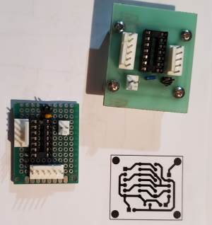
As I also do 3D printing, I use Fusion for designing enclosures and many other items but not yet used it for PCB layout. I have never found KiCad lacking in any area. Almost everything I do involves SMD’s. I can make boards to support 0802 but most of the time I try to stick with 1206 size. One, this size is reasonably easy to work with and second, I have a good selection of SMD’s in that size. Equipment-wise I am also well set up for SMD work including a stereo microscope which makes them easy to work with and easy on the old eyes. Another technique I like is to make generic plug-in carrier PCB boards using Amazon parts – sockets, pins etc. Larger DIP IC’s are hard come by these days but surface mount IC’s are cheaper and readily available. Then I plug these carrier boards into a small motherboard and use wire-wrapping for interconnects. Changes are easy so this method lends itself well to prototyping.
View attachment 77971
Nicely done. As in really beautiful!
I originally built my JGRO CNC router to do PC boards but it was just to wobbly for that. I have linear bearings for it so eventually I may go there with that. Meanwhile I get the PC boards done in China and the layouts are done with Protel 99SE or if I really have to, with Altium.

I have used laser printer transfer methods and then etch.
1770750925942.png
 
Nicely done. As in really beautiful!
I originally built my JGRO CNC router to do PC boards but it was just to wobbly for that. I have linear bearings for it so eventually I may go there with that. Meanwhile I get the PC boards done in China and the layouts are done with Protel 99SE or if I really have to, with Altium.

I have used laser printer transfer methods and then etch.
Thanks! I used to etch but the off gas rusted a lot of my equipment. I seem to recall it was ferric chloride but not done that in many moons.
re China PCB's - a wise friend told me "never pay $5. for a board when you can make your own for $2000.".
 
I’m a bit late to the party but thought I’d share my experiences regarding PCB making and workflow with my electronic projects. I make all my own PCB’s myself using the isolation routing method. I initially joined this group to learn as much as I could about CNC machining as my objective was to build up a system to make PCB’s and some smaller metal parts for RF projects. I built up a CNC controller from scratch based on an Arduino controller running GRBL firmware and I use a Sherline mill & isolation routing to machine my boards. I have made many boards using this technique, mostly double sided. I begin the process by entering my schematic design in the circuit simulator LTspice. I spend a lot of time here optimizing it and when I have it working well enough, I take the schematic into KiCad to do the board layout. I spend a lot of time at this phase too since I try to not only optimize circuit layout but also attempt to use as many of the parts that I have on hand. This usually involves building custom footprints. Typically, everything I do is a one-off. When I’m happy with the layout, KiCad outputs the Gerber and drill files. I take these into another app called FlatCam which produces the g-code. These are loaded into a PC running an application called bCNC. This is connected to the Arduino and the CNC XYZ controllers via an RS232 serial port. After origin settings for XYZ are zeroed, I turn on the mill and hit start.

As I also do 3D printing, I use Fusion for designing enclosures and many other items but not yet used it for PCB layout. I have never found KiCad lacking in any area. Almost everything I do involves SMD’s. I can make boards to support 0802 but most of the time I try to stick with 1206 size. One, this size is reasonably easy to work with and second, I have a good selection of SMD’s in that size. Equipment-wise I am also well set up for SMD work including a stereo microscope which makes them easy to work with and easy on the old eyes. Another technique I like is to make generic plug-in carrier PCB boards using Amazon parts – sockets, pins etc. Larger DIP IC’s are hard come by these days but surface mount IC’s are cheaper and readily available. Then I plug these carrier boards into a small motherboard and use wire-wrapping for interconnects. Changes are easy so this method lends itself well to prototyping.
View attachment 77971
What tool bit do you use for cutting the PC board routes?
 
Hello team. Something might be useful to share with you, folks.

I assembled TDRO adapter based on original schematics and ESP32 DEVKIT V1. It is smaller board with a different pin layout - that is what i had at the moment. I also developed FW (ino file) for the ESP32 that is mimicking linear scales and sends test signals to the tablet with installed TDRO application. It works without any scales and buffers - just a test between ESP32 and application via bluetooth.
Next , I went ahead and added three quadrature encoders reading support, tacho interrupt and touch probe interface. Now it looks like fully functional TDRO adapter with BT to connect to the tablet.
* Board: ESP32 Dev Module (DOIT ESP32 DEVKIT V1)
*
* Pin assignments:
* X encoder: GPIO 34 (A), GPIO 35 (B)
* Y encoder: GPIO 32 (A), GPIO 33 (B)
* Z encoder: GPIO 25 (A), GPIO 26 (B)
* Touch probe: GPIO 27 (active LOW, internal pull-up)
* Tachometer: GPIO 14 (1 pulse/rev, falling edge interrupt)
* Blue LED: GPIO 2 (built-in)

I am not sure if that is fully legal - I just had a protocol of the exchange between adapter and tablet - openly available in the internet - and I developed code myself (with tiny help from Claude. 🙂 ) . If somebody need it for debugging his board, scales or for studying purposes, I can share it.
 
E117-01 are the boards I got made.

As for esp32's people can buy them directly from Yurhi and they come programmed.
I am looking at getting some 38 pin esp32's off amazon, and then will compare the pinout's to the ones needed for the boards. When I get them I will post if they will work or not.

I have 10 of the boards here. I will be honest with everyone. I will not likely be able to test these until the fall. I will send boards to any wanting some. With the postal strike up and downs, I am not sure if and when we can get them to people. But I will get them in the mail as soon as possible for those that want them.
Hi, I started to research how to build DRO on budget and found this forum. And from here jumped to TouchDRO web site. With experience I have in ESP, I did not take long to program one with touchdro-free-v3.2. And now need to build electronics. Djberta, you mentioned that may be some bare PCBs rev. E117-01 are available? Could you please PM me what would take to get one? I'm in Texas, 75075. Thank you.
 
Back
Top