
Nicely done. As in really beautiful!I’m a bit late to the party but thought I’d share my experiences regarding PCB making and workflow with my electronic projects. I make all my own PCB’s myself using the isolation routing method. I initially joined this group to learn as much as I could about CNC machining as my objective was to build up a system to make PCB’s and some smaller metal parts for RF projects. I built up a CNC controller from scratch based on an Arduino controller running GRBL firmware and I use a Sherline mill & isolation routing to machine my boards. I have made many boards using this technique, mostly double sided. I begin the process by entering my schematic design in the circuit simulator LTspice. I spend a lot of time here optimizing it and when I have it working well enough, I take the schematic into KiCad to do the board layout. I spend a lot of time at this phase too since I try to not only optimize circuit layout but also attempt to use as many of the parts that I have on hand. This usually involves building custom footprints. Typically, everything I do is a one-off. When I’m happy with the layout, KiCad outputs the Gerber and drill files. I take these into another app called FlatCam which produces the g-code. These are loaded into a PC running an application called bCNC. This is connected to the Arduino and the CNC XYZ controllers via an RS232 serial port. After origin settings for XYZ are zeroed, I turn on the mill and hit start.
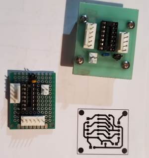
As I also do 3D printing, I use Fusion for designing enclosures and many other items but not yet used it for PCB layout. I have never found KiCad lacking in any area. Almost everything I do involves SMD’s. I can make boards to support 0802 but most of the time I try to stick with 1206 size. One, this size is reasonably easy to work with and second, I have a good selection of SMD’s in that size. Equipment-wise I am also well set up for SMD work including a stereo microscope which makes them easy to work with and easy on the old eyes. Another technique I like is to make generic plug-in carrier PCB boards using Amazon parts – sockets, pins etc. Larger DIP IC’s are hard come by these days but surface mount IC’s are cheaper and readily available. Then I plug these carrier boards into a small motherboard and use wire-wrapping for interconnects. Changes are easy so this method lends itself well to prototyping.
View attachment 77971
I originally built my JGRO CNC router to do PC boards but it was just to wobbly for that. I have linear bearings for it so eventually I may go there with that. Meanwhile I get the PC boards done in China and the layouts are done with Protel 99SE or if I really have to, with Altium.
I have used laser printer transfer methods and then etch.