mickeyf
Ultra Member
When did that happen, and how did I sleep through it?
A Loooong time ago! And sadly, I still have a pile of blank copper clad board which must still be good for something?
When did that happen, and how did I sleep through it?
Well hold onto yer socks. SPICE is included with Fusion360. (Its fabulous GIGO software!)A million years ago I used a program called spice to do that sort of thing. It ran on CPM. I did a quick search and see dozens of modern take-offs. LTSpice, PSpice, NGSpice to name a few. Google them. They are all sorta what you are looking for.
Just remember - garbage in, garbage out. It's always a challenge to create an input signal that looks like the real world signal your circuit will actually see. But you can always try extremes to test it.
I will look into this and make the changes before I send you the schematic.You asked for suggestions and I have expertise in this area, I have designed many hundreds of complex boards so realize when I look at a circuit/layout I look at it critically.
0) The regulators are missing decoupling and may well oscillate, depending on type used.
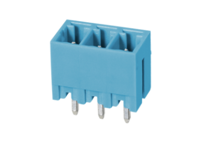
I will be running wires up from these connectors to a DB9 socket. I did this just because the DB9s are too large to mount right on the board.1) I would replace the terminal blocks with plugable ones. They are inexpensive.

Connections will be to DB9 plugs mounted above the board, so not leaving the enclosure. Thought this woudl be easier than wires coming between wall and socket. This will change when I change to plug in terminals.2) Wire opening should face outside edges.
The nice thing about through mount is as long as the holes are in line and don't cross other components, I can mount them in holes that are between about 8 mm and 40 mm apart. 😉3) I work from extensive proven libraries so I don't have to worry about things like incorrect pad hole size, that's just one (of many) problems you might encounter when using unproven libraries, or creating your own footprints. I would verify.
Had to look up this acronym. I went with the Fusion default settings. They know more about this than I do. (The janitor at Autodesk likely knows more than I do). I"ll do more digging.4) I don't use fusion, so I don't know how well the DRC works or how you have configured it?
Will send to you. It is the same schematic Yuriy designed and posted at https://www.touchdro.com/resources/adapters/diy/esp32-diy-dro.html but I added the 5V, 3.3V, LED, socket for switch and 12V plug.5) I can't clearly see the schematic, can you post a higher resolution version.
You bet I will! Thanks!6) Might want to check out AllPCB, they often have coupons for free small boards like this for new customers.
If I get these two working, that would be a great next step.7) Through holes components are 1980's technology, SMT uses a fraction of the space, and should allow you to accomplish #2 above
I assumed Yuiy knew where to put them. I have added 100uF to the +5v and +3V3 outs and to ground. When you say they are not in the right place, do you mean in the schematic, or the physical placement on the board? I think I got the schematic right on the scale inputs, but I certainly could be wrong, or Yuriy could have made a mistake.8) Your decoupling capacitors are not where they should be.
Will be trying to figure out how to do a ground plane. I soul also look at the traces to the scales, as they9) Are you using a ground plane or just traces for ground? If traces how wide are they and have you considered the ground path?
I thought I might be breadboarding it and no further. Also easier to take up spacing errors. SMT is within my skill level for soldering, so maybe next time.10) auto-routers are cool to watch, but they generally result in a terrible layout.
11) Hand soldering a SMT version of that board would be trivial if you use 0603 min.
I agree., In this case the circuit is easy, and there are only 3 resistor values (two really, and one outlier) and they are grouped by type, so no searching needed on this one.12) Good practice is to re-annotate the component designators in a logical fashion so you don't have to hunt.
Great idea! Once I learn how to label in Fusion.13) Label individual terminal block signals
The chips are notched, which I think will print, and the ESP32 is orientated with the antenna to the outside of the board. (seemed like a good idea to me)14) I don't see pin 1 indicators on silkscreen.
I appreciate you taking the time to give these suggestions! I have a feeling I couldn't afford you.= normally.15) There is more, but I will stop, I'm a bit picky because my last job was as a consultant "fixing" stuff like this for others.

Excellent information! I'll work on the things you suggested. I'm enjoying the challenge and learning involved.0) Cap should be as physically close as possible to the regulator terminals. This is where SMT makes your life a lot easier,
1) Plugable connector, perfect that's exactly the type I was thinking of. There are two types; the ones with the rising cage clamp are more user friendly than the cheap leaf spring type
2) Yes it will, although placing the DB's directly on the board, saves time, lowers cost and reduces failure points
3) The common error is having the hole size the same size as the pin and then after the PCB house "plates up" the hole, the hole is now too small.
4) A good DRC engine is priceless, this may sound like I'm exaggerating, but I'm not.... when I first complete a layout I run the DRC and it's very common to have a hundred or so errors flagged. If I did a good job these are mostly cosmetic, like silkscreen too close to pad, or some generic spacing error, that when you fix the offending component, 20 errors go away at once. The big one to be aware of is when you use nets to describe signals and then call one say 3v3 and the other 3V3, these are treated as different nets and so if not connected will not flag an error.
9) When I do a layout the first step is to layout the ground and power traces. For complex boards muti-layer boards this is easy because you dedicate an entire layer to say ground, and another for 3v3 etc, but with a two layer board, its best to dedicate one layer to (for the most part) to be used for ground and Vcc so a solid plane for the ground with the VCC traces within that ground plane, and then use the other layer for your signals. I will show an example below. This is a very simple low speed design so decoupling and ground planes are not super critical, however this circuit will be working in a potentially noisy (electrically) environment. I have fixed countless designs (some in production) that work fine on the bench (everything is connected correctly), however the moment the device is asked to work in the real world it becomes flaky.
10) SMT is your friend
I'm retired, more than happy to help, everyone can afford free;-)
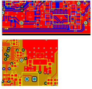
Two examples showing ground plane and regulator decoupling:
Top example is a two layer board, U5 is a 3 terminal regulator. The bottom blue plane is (for the most part used for ground) and is a solid plane. That same ground is repeated on the top layer where possible. Note C4 and C25 and how they have very short connections to both ground and their voltage terminals
Bottom example is a 4 layer board, the gold plane (mid layer 1) is ground, and the (not shown 3v3 Midlayer 2 is everywhere. Note C7 and C8 and their close proximity to U3
The important point that is often overlooked by electronic hobyists is that they think in "DC" terms, I need to connect pin 1 to ground, I have a trace to ground so I'm good. Now appreciate that the digital signals are not DC they are AC and can change very rapidly << a micro-second, and long narrow long traces have inductance, that inductance will not allow those signals to change quickly, will effectively act as a resistor (if you think in DC terms), so will change the signal level and generate noise during the transition. With very high speed GHz designes (for example the QorIQ above), nothing would work without proper ground planes, even the countless signal traces to things like memory have to have matched lengths so the signals arrive at the same time, it makes for a tricky layout.
View attachment 53838
Socket is a great idea. I didn't do that. And thanks fro the tip on the ground plane.Tom make sure that your ground plane does not extend under the esp32 antenna section if your using blue tooth or wifi. It can diminish your wireless distance. I usually try to make my ground plane as large as possible. In easyeda you can set it to just that. Not sure with fusion. I didn’t see if you socketed the esp32, so you can swap out the esp32 if you have issues.
Looks like it is coming together great. excited to see how your design works out. I put mine to the back burner some time ago.
Except I think a classroom setting might work better than the scatter-gun approach of Youtube.
.....
Of course, the best teacher of all is experience.
The Magic Smoke is known by many names. Experience is just one of them.......Many a lesson has been learned by the release of the magic smoke 😀
The Magic Smoke is known by many names. Experience is just one of them.......
Also the aroma of popping electroylic capacitors 😀
When I majored in electronics in highschool a few of the guys made sport of it, lol
Yup, I duct tape all vent holes on anything I initially wire up these days, it prevents the magic smoke from escaping....... 🙄 😉Many a lesson has been learned by the release of the magic smoke 😀
Although I have not used it the fusion electronics module it is supposed to be quite good. I have a friend who makes custom power supplies. He does it all with fusion. He resents that he has to pay for the CAD/CAM part of fusion because he considers it to be useless.Holy Crap I feel old......
Home software like Fusion 360 will draw circuits and then make pcboard layouts?
For serious? When did that happen, and how did I sleep through it?
I thought 3D printing was amazing. This is mind blowing. It is like Black Magic.....
What is the process between making the layout and etching an actual Copper Board?


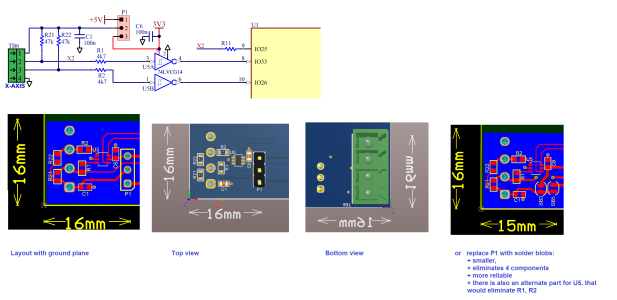
Man, what a difference it makes when you know what you are doing! SMT also offers a lot more flexibility on a smaller footprint.The fun part of electronic design is that there are so many ways to accomplish any particular design.
Here are a couple of possibilities that will only require about half your available board space and use less components.
I would actually replace TB6 with the DB and eliminate all the hoopla associated with the terminal block to DB wiring, you have enough room.
I'm not sure if Fusion imports Altium files, if it does your welcome to the files for these examples.
BTW with your original schematic. if the intent was to power the board with 5V, your circuit won't work.
View attachment 53875
