• Scam Alert. Members are reminded to NOT send money to buy anything. Don't buy things remote and have it shipped - go get it yourself, pay in person, and take your equipment with you. Scammers have burned people on this forum. Urgency, secrecy, excuses, selling for friend, newish members, FUD, are RED FLAGS. A video conference call is not adequate assurance. Face to face interactions are required. Please report suspicions to the forum admins. Stay Safe - anyone can get scammed.

Schematics and Circuit Board layout with Fusion 360

Tomc938

Ultra Member
Premium Member
I have my esp32 dev boards flashed and working with my Tablet - it connects anyway.

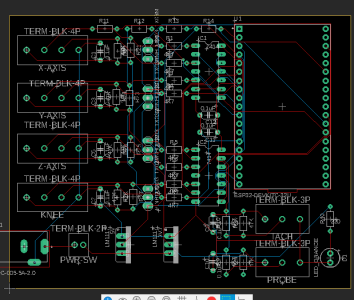
I spent the last two days using Fusion 360 electronics project design to reproduce Yuriy's schematic for the ESP32 scale adapter (https://www.touchdro.com/resources/adapters/diy/esp32-diy-dro.html) and figuring out how to find components, define components, place components (in the schematic and the PCB board) and all the other little things I needed to learn to use Fusion 360. Some things were not intuitive - once you choose a component, you hit "return" and then you can place the component. No click and drag option. but I gotta say, when it comes to figuring out the traces for the PCB board, Fusion is a thing of beauty! I deleted the traces and had it re-wire things for me a few times. Sometimes because I made significant changes in components and layout, and sometimes just for the fun of watching it work.

I added 3.3 and 5v power, and LED to show when the unit is on, and switch to turn it on (and off - I thought of everything).

I a not sure what kind of connectors I will use. Yuriy suggests DB9, but the free version of Fusion only allows a maximum of 100 mm x 100 mm PBC, and there wasn't room on the back. So I went with small terminal blocks I can wire them, or whatever kind of connector I decide to use, after the board is built.

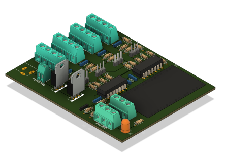
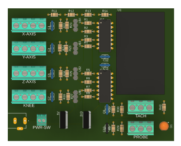
So here's the 3D rendering of the board. I'm open to any positive suggestions anyone may have. It's gone through a lot of revisions and I may do a few more tweaks before getting the boards made. I have enough material to make 2 adapters. One for my milling machine snd one for my lathe. Both will just have X and Y axis for now, but I can add more at any point. Screenshot 2024-11-02 at 6.30.34 PM.pngScreenshot 2024-11-02 at 6.30.56 PM.pngScreenshot 2024-11-02 at 6.34.27 PM.pngScreenshot 2024-11-02 at 6.34.09 PM.png
 
Very nice Tom. I use easyeda then import to jlcpcb. I have not had luck with fusion. Auto desk bought eagle years ago. So fusion is completely capable. It’s all meat this point. I partial made the same board then changed careers so it’s all been on hold for more than a year. We both seem to have been on the same track.

What scales are you looking to use? In my experience it’s better to have the end use connectors rather the terminals. Like db9 connectors or usb type A. I have had trouble with the screw terminals over the years on dif projects but it’s more subjective then an overall issue.

If your fabbing through one of the houses like jlcpcb or Pcb way maybe look at going to surface mount for the minor components. It’s very cost effective and reliable. For about 5 years I’ve been using surface mount more and more. So much easier to solder, better heat, better price. I have been surprised a couple times on the price of having one of the houses do the surface mount components.
 
looks good

i would turn the terminal blocks 90deg if you intend to keep those, easier to wire up, and the lm117's look tight for heat sinks, i might consider turning them 90 deg as well

ive also use easyEDA the odd time i do a project like this, pretty simple to use, no size limits

i like smd's, take up much less space and can be cheaper, next project im going to try smd's with the solder paste and a heat gun....i find it kind of tricky doing multiple pins of an smd with a soldering iron
 
i like smd's, take up much less space and can be cheaper, next project im going to try smd's with the solder paste and a heat gun....i find it kind of tricky doing multiple pins of an smd with a soldering iron
Do it in the oven! When ordering the PCB also order a stencil. Use a squeegee and solder paste to populate the copper with solder paste. With tweezers and a careful touch, place the SMT components gently on their pads. Then in a toaster oven set for approx 220 degrees, bake that cookie for about 3 minutes. Or better still use a PID controller to control the oven to preheat-soak-cooldown according to the solder spec.

I've been making SMT boards for CNC and PLCs based on the Teensy 4.1 directly from Eagle (now assimilated into Fusion360) using OSHPark and OSHStencils in the US (3 week turnaround) and more recently with PCBway in Shenzhen (1 week turnaround). As others have said it is very cost effective for the board manufacturers to populate the tiny SMT parts when the run is 10 or more boards, but for a proto board or two, the stencil route is easier.
 
You asked for suggestions and I have expertise in this area, I have designed many hundreds of complex boards so realize when I look at a circuit/layout I look at it critically.

0) The regulators are missing decoupling and may well oscillate, depending on type used.
1) I would replace the terminal blocks with plugable ones. They are inexpensive.
2) Wire opening should face outside edges.
3) I work from extensive proven libraries so I don't have to worry about things like incorrect pad hole size, that's just one (of many) problems you might encounter when using unproven libraries, or creating your own footprints. I would verify.
4) I don't use fusion, so I don't know how well the DRC works or how you have configured it?
5) I can't clearly see the schematic, can you post a higher resolution version.
6) Might want to check out AllPCB, they often have coupons for free small boards like this for new customers.
7) Through holes components are 1980's technology, SMT uses a fraction of the space, and should allow you to accomplish #2 above
8) Your decoupling capacitors are not where they should be.
9) Are you using a ground plane or just traces for ground? If traces how wide are they and have you considered the ground path?
10) auto-routers are cool to watch, but they generally result in a terrible layout.
11) Hand soldering a SMT version of that board would be trivial if you use 0603 min.
12) Good practice is to re-annotate the component designators in a logical fashion so you don't have to hunt.
13) Label individual terminal block signals
14) I don't see pin 1 indicators on silkscreen.
15) There is more, but I will stop, I'm a bit picky because my last job was as a consultant "fixing" stuff like this for others.
 
Last edited:
Very nice Tom. I use easyeda then import to jlcpcb. I have not had luck with fusion. Auto desk bought eagle years ago. So fusion is completely capable. It’s all meat this point. I partial made the same board then changed careers so it’s all been on hold for more than a year. We both seem to have been on the same track.

What scales are you looking to use? In my experience it’s better to have the end use connectors rather the terminals. Like db9 connectors or usb type A. I have had trouble with the screw terminals over the years on dif projects but it’s more subjective then an overall issue.

If your fabbing through one of the houses like jlcpcb or Pcb way maybe look at going to surface mount for the minor components. It’s very cost effective and reliable. For about 5 years I’ve been using surface mount more and more. So much easier to solder, better heat, better price. I have been surprised a couple times on the price of having one of the houses do the surface mount components.
Thanks!

I'll be using Accurite 5 scales on my mill and Metric 0.01 (I think they are also Accurite) on my lathe.

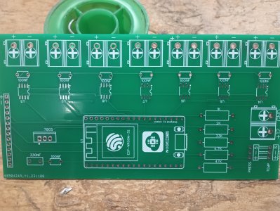
I thought about surface mount. I can solder these by hand. (see attached) but I wanted to work with something bigger the first time as I wasn't sure I could figure out/know how to use Fusion. Now that I have done this it would be easy to switch out the through hole components for surface mount in the schematic and then rearrange them on the board. They would give a smaller footprint.

I'll be looking at getting boards made next. It's been a fun journey and I've learned lots.
 
looks good

i would turn the terminal blocks 90deg if you intend to keep those, easier to wire up, and the lm117's look tight for heat sinks, i might consider turning them 90 deg as well

ive also use easyEDA the odd time i do a project like this, pretty simple to use, no size limits

i like smd's, take up much less space and can be cheaper, next project im going to try smd's with the solder paste and a heat gun....i find it kind of tricky doing multiple pins of an smd with a soldering iron
I think I tried the terminal blocks the other way and I think there wasn't room.
You asked for suggestions and I have expertise in this area, I have designed many hundreds of complex boards so realize when I look at a circuit/layout I look at it critically.

0) The regulators are missing decoupling and may well oscillate, depending on type used.
1) I would replace the terminal blocks with plugable ones. They are inexpensive.
2) Wire opening should face outside edges.
3) I work from extensive proven libraries so I don't have to worry about things like incorrect pad hole size, that's just one (of many) problems you might encounter when using unproven libraries, or creating your own footprints. I would verify.
4) I don't use fusion, so I don't know how well the DRC works or how you have configured it?
5) I can't clearly see the schematic, can you post a higher resolution version.
6) Might want to check out AllPCB, they often have coupons for free small boards like this for new customers.
7) Through holes components are 1980's technology, SMT uses a fraction of the space, and should allow you to accomplish #2 above
8) Your decoupling capacitors are not where they should be.
9) Are you using a ground plane or just traces for ground? If traces how wide are they and have you considered the ground path?
10) auto-routers are cool to watch, but they generally result in a terrible layout.
11) Hand soldering a SMT version of that board would be trivial if you use 0603 min.
12) Good practice is to re-annotate the component designators in a logical fashion so you don't have to hunt.
13) Label individual terminal block signals
14) I don't see pin 1 indicators on silkscreen.
15) There is more, but I will stop, I'm a bit picky because my last job was as a consultant "fixing" stuff like this for others.
Thanks for all the suggestions! I really do appreciate it. I have minimal electronics training.

I'll see if I can DM you the schematic and board layout.

And I'll ask for further clarification on the points where I have to look up words to know what you're saying. (not quite that bad, but it is late)
 
I spent the last two days using Fusion 360 electronics project design to reproduce Yuriy's schematic for the ESP32 scale adapter

Holy Crap I feel old......

Home software like Fusion 360 will draw circuits and then make pcboard layouts?

For serious? When did that happen, and how did I sleep through it?

I thought 3D printing was amazing. This is mind blowing. It is like Black Magic.....

What is the process between making the layout and etching an actual Copper Board?
 
What is the process between making the layout and etching an actual Copper Board?
Layout is followed by Gerber, drill file and Pick & Place file generation, just a few clicks and it's done.

Small PCB like this are priced about $2 per board (qty 10)+shipping manufactured from ALL, JLC etc. They usually ship within a few days and arrive within a week, and the quality will far surpass what you will ever accomplish at home. The raw materials to etch a board would eclipse these delivered prices by a large margin. Small PCB houses in Canada have either closed or specialize in quality or preserving IP. AP circuits in Alberta was for years the go-to quick, cheap PCB house. They folded about 10 years back.
 
Last edited:
Holy Crap I feel old......

Home software like Fusion 360 will draw circuits and then make pcboard layouts?

For serious? When did that happen, and how did I sleep through it?

I thought 3D printing was amazing. This is mind blowing. It is like Black Magic.....

What is the process between making the layout and etching an actual Copper Board?

you should give one of them a go,

the first time i tried one it was like magic, make schematic, hit the button to generate, BAM turns that into a pcb layout, you then move things around to where you want, it does the routing, fricking amazing, and free, most of them will even generate a BOM that you can upload and it will order the parts as well

Magic, pure magic
 
The easiest route to go with basically no install. Easyeda then import in to jlcpcb or Pcb way, make sure the boards look good, order the smd mask if smd. Hit go, clip coupon I always seem to have a 5 dollar off coupon, pay. Week later 5 boards. Also check the libraries. Lots of people post their designs. I got a 2 stepper driver card for an Arduino mini, worked great.

Like others have said you need to watch the libraries.

As for etching. I have seen online an easy way. Once your design is done. You use a laser, paint the copper, burn off the paint to expose the copper then etch. Sure beats the old days of ironing on or uv exposure.

Slow poke beat me lol
 
Holy Crap I feel old......

Home software like Fusion 360 will draw circuits and then make pcboard layouts?

For serious? When did that happen, and how did I sleep through it?

I thought 3D printing was amazing. This is mind blowing. It is like Black Magic.....

What is the process between making the layout and etching an actual Copper Board?
I KNOW! And it sounds like Fusion isn't the only one that works this magic.

AS far as board production, it sounds like you send the file to some board place and they send you the board back. There are lots of places online and some suggestions here I am going to check out. One place I did a quick and dirty quote with was going to be $14 for 5 boards including shipping. I only need 2, but at that price...
 
The raw materials to etch a board would eclipse these delivered prices by a large margin.

Not a problem here. I still have everything I would need to etch a board right here right now the old fashioned way.

That minimum order of 10 would be a waste for a guy like me. I ain't building more than one of anything.

Then again....... A prototyping board with a breadboard socket and screw terminals would be handy......
 
Not sure how vias work with home etching?
I don't think home etching of this board is going to happen at home, that u has about one thousand pins with 0.5mm spacing...
 
Last edited:
Here is the last batch of boards I had made, I don't recall if it was pcb way or express pcb

You can also get other colors, black, green, blue, etc etc, stenciled in whatever color, multi layers, it's worth the coin for a long lasting project

I could never make a board this nice by hand

IMG_20241103_121750124.jpg
 
Bit of a tangent question but do you guys have resources for electronics simulation software? Like when you design circuits & want to test what it will actually do, do you start with a different app vs the board production side of it? I've only dabbled in electronics & built the odd hobby project entirely based on other peoples designs. Maybe I'm naïve because the subject is so broad, but was thinking this might be a way of accelerating learning vs. textbooks & how-to books.
 
Bit of a tangent question but do you guys have resources for electronics simulation software? Like when you design circuits & want to test what it will actually do, do you start with a different app vs the board production side of it? I've only dabbled in electronics & built the odd hobby project entirely based on other peoples designs. Maybe I'm naïve because the subject is so broad, but was thinking this might be a way of accelerating learning vs. textbooks & how-to books.

I still breadboard things, although these days most of the heavy lifting is done with some form of microcontroller. Most of the external circuitry is simple and a lot of the more popular things you can buy a "module" for, literally just connect wires to pins. Replace the thought of doing electronics with the idea of coding....with a little bit of electronics to support it
 
Ya, my friend gave me some YouTube video recs on Arduino which I started watching until life got in the way. Very interesting & probably in my future with more time on my hands for the reasons you mention. Even that so called narrow subject of controllers is a rabbit hole. I rather suspect general electronics might just be too broad for any piece of software. But maybe I should have dumbed down my question to Basic Electronics - resistors, capacitors, transformers... that sort of thing. Seems to me I saw something like this years ago, like a digital breadboard. But maybe it was bootleg of industrial software at the time.
 
But maybe I should have dumbed down my question to Basic Electronics - resistors, capacitors, transformers... that sort of thing. Seems to me I saw something like this years ago, like a digital breadboard. But maybe it was bootleg of industrial software at the time.

A million years ago I used a program called spice to do that sort of thing. It ran on CPM. I did a quick search and see dozens of modern take-offs. LTSpice, PSpice, NGSpice to name a few. Google them. They are all sorta what you are looking for.

Just remember - garbage in, garbage out. It's always a challenge to create an input signal that looks like the real world signal your circuit will actually see. But you can always try extremes to test it.
 
Back
Top