• Scam Alert. Members are reminded to NOT send money to buy anything. Don't buy things remote and have it shipped - go get it yourself, pay in person, and take your equipment with you. Scammers have burned people on this forum. Urgency, secrecy, excuses, selling for friend, newish members, FUD, are RED FLAGS. A video conference call is not adequate assurance. Face to face interactions are required. Please report suspicions to the forum admins. Stay Safe - anyone can get scammed.
  • Several Regions have held meetups already, but others are being planned or are evaluating the interest. The Calgary Area Meetup is set for Saturday July 12th at 10am. The signup thread is here! Arbutus has also explored interest in a Fraser Valley meetup but it seems members either missed his thread or had other plans. Let him know if you are interested in a meetup later in the year by posting here! Slowpoke is trying to pull together an Ottawa area meetup later this summer. No date has been selected yet, so let him know if you are interested here! We are not aware of any other meetups being planned this year. If you are interested in doing something in your area, let everyone know and make it happen! Meetups are a great way to make new machining friends and get hands on help in your area. Don’t be shy, sign up and come, or plan your own meetup!

Tips/Techniques Ever wondered how PCB boards are made?

Tips/Techniques

Arbutus

Ultra Member
Premium Member
I came across this very well written article describing the processing steps behind a modern microcircuit PCB, it's well worth a read.

Summit PCB production

We have come a long way from Letraset rub-on resist traces and ferric chloride! My latest set of boards (from a different supplier) are 4 layers SMT with 6mil traces. The total turnaround from order to delivery was 5 days including shipping from Asia to Canada. Amazing!
🙂
 
We have come a long way from Letraset rub-on resist traces and ferric chloride!

I have several drawers of that old circuit board making equipment and supplies. I think what you are suggesting is that I should just pitch it...... I guess it's time has passed.

While we are on the subject, what is the best way to make a normal sized board today for components that are big enough that you can still see the colour code on them with one old naked eye?
 
Wondering, who was that supplier ? Is that hobbyists friendly ? Mind to share ?
Recently I have been using two suppliers - PCBway and SeeedStudio. Very similar services and options. They handle orders from 1 board to mass production and can assemble, test and package too if thats needed.

And to answer @Susquatch's question - a 2 layer PTH board can be made by any manufacturer if the Gerber files are available. Some suppliers also accept Altium, KiCad and Eagle (Fusion360) board files directly, so that saves the Gerber step. F360 has a fairly comprehensive component library now with SMT and PTH parts, and the autorouter handles up to 16 layer boards, so thats all available too.

If you want to make your own - there is a laser printer transfer process where you iron the print onto the copper, etch, then drill. Good for 1 sided boards due to front/back alignment issues, but it will get you started.
 
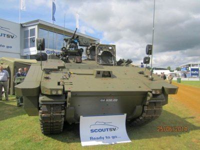
@jcdammeyer - I love it!

1755058405596.png

I wanna plow with one of those and I could care less how it is wired!
 
I have several drawers of that old circuit board making equipment and supplies. I think what you are suggesting is that I should just pitch it...... I guess it's time has passed.

While we are on the subject, what is the best way to make a normal sized board today for components that are big enough that you can still see the colour code on them with one old naked eye?
I use DipTrace for schematic and layout. Way back when KiCad was almost uselss I had a need and haven't bothered switching again. But were I to start over it would be KiCad.
PCBWay has excellent facilities, I look for suppliers in Canada but can't justify the expense.
 
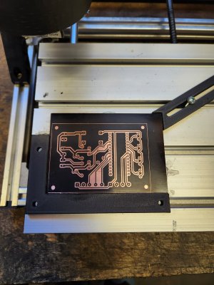
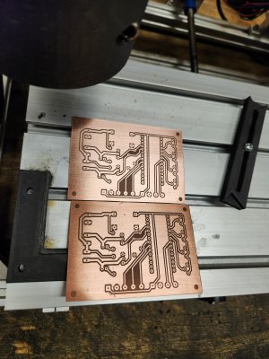
Only making simple things, but Kicad and Lightburn. I coat the boards with paint, burn the outline of the traces with a 5w hobby laser on a 3018, then etch. Makes for pretty quick in-house prototyping. A silk screen works pretty well for applying and even layer of UV cured solder mask...burn the pads off with the laser.
 

Attachments

  • 20241229_140848.jpg
    20241229_140848.jpg
    1.3 MB · Views: 8
  • 20241229_200210.jpg
    20241229_200210.jpg
    1.6 MB · Views: 9
Can you 3d print boards? At home? with a filament switcher for swapping insulating layers and copper infused filament for the traces? and print the via's with the copper filament?
 
Back
Top